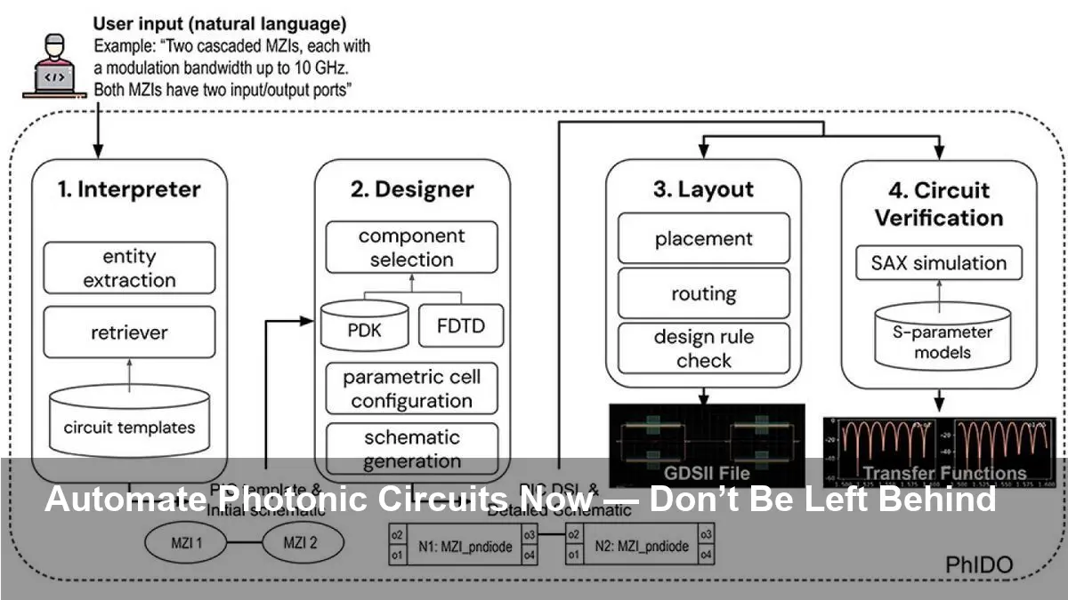
• Large language models can translate natural-language instructions into usable photonic circuit schematics.
• The AI-driven tool aims to speed design, reduce repetitive work, and lower the barrier for nonexpert users.
• Technical challenges remain: fabrication constraints, simulation validation, and human-in-the-loop verification.
AI tool converts text into photonic circuit designs, promising faster workflows
Researchers highlighted by the American Institute of Physics (AIP) have developed an AI-driven approach that uses large language models (LLMs) to automate parts of photonic circuit design. The system interprets plain-language instructions and generates functional schematic representations of photonic circuits — a step that could dramatically speed design cycles and open photonic engineering to more users.
What the tool does
Instead of hand-drawing layouts or translating formal specifications directly into schematics, designers can tell the AI what they want in natural language — for example, “build a wavelength demultiplexer for telecom bands” — and receive a schematic-ready output. Early demonstrations show the model can produce usable circuit diagrams that capture intended components and interconnections, reducing repetitive manual drafting and accelerating prototyping.
Why this matters
Photonic circuits — which manipulate light on-chip for communications, sensing, and emerging optical computing — typically require specialized expertise to design. Automating the conversion from concept to schematic promises several benefits:
- Faster iteration: Designers can explore more variants quickly.
- Lower barrier to entry: Nonexperts and multidisciplinary teams can participate earlier.
- Reduced tedium: Repetitive layout and wiring tasks can be offloaded to the AI, letting engineers focus on higher-level decisions.
Social proof for the approach comes from the broader success of LLMs in code generation and design tasks in other fields, suggesting similar gains are achievable in photonics.
Remaining challenges and risks
The researchers — and AIP’s coverage — emphasize that the tool is not a fully autonomous designer. Critical hurdles include:
- Physical and fabrication constraints: Generated schematics must respect manufacturing rules and material limits.
- Simulation and verification: Outputs require optical simulation to validate performance and identify hidden faults.
- Generalization and safety: The model must avoid proposing nonfabricable or unsafe configurations.
A human-in-the-loop workflow remains essential. Experienced engineers are still needed to vet, adapt, and validate AI-generated designs before fabrication.
What’s next
Future development will likely integrate fabrication rules, tighter coupling with simulation engines, and expanded training datasets to improve reliability. If these improvements succeed, the tool could become part of standard photonic design toolchains, enabling faster research and commercial product development in optical communications, sensors, and on-chip photonics.
Adoption will depend on proving robust, repeatable results across many device classes and on creating clear verification workflows so teams can trust AI-assisted schematics.
For now, the message is clear: AI can already translate intentions into schematics, but careful verification and continued engineering oversight remain nonnegotiable as the technology moves from promising demonstrations to everyday engineering practice.
Image Referance: https://www.aip.org/scilights/creating-an-ai-driven-tool-to-automate-photonic-circuit-design
